

Future Trend of Metrology & Inspection:
Frontier Insights from a Device Maker, an Equipment Supplier, and Academia
Dec 9 to 11, 2026 | Tokyo Big Sight
What is Metorology & Inspection Summit?
In semiconductor manufacturing, which underpins progress in the AI era, integration technologies like miniaturization and chiplets are accelerating. However, achieving this requires advanced inspection and metrology technologies.
While these technologies are critical to the industry, there is significant opportunity to further enhance their visibility and recognition.
The Metrology & Inspection Summit fosters advancement in metrology and inspection technologies and promotes collaboration to address shared industry challenges. This initiative shines a spotlight on the essential technologies that underpin the future growth and innovation of the semiconductor industry.
Join Metorology & Inspection Summit
Exhibition
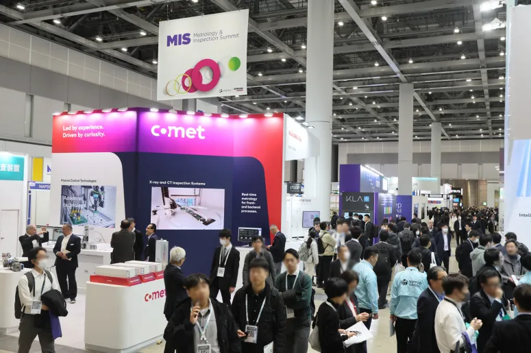
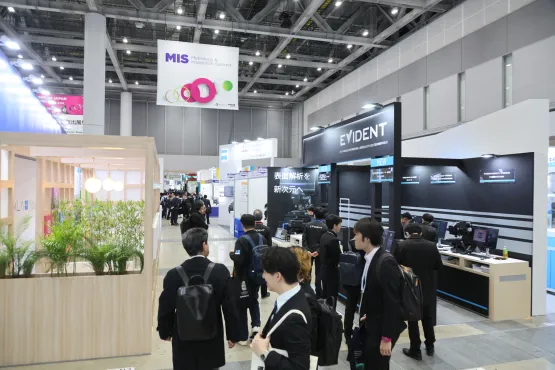
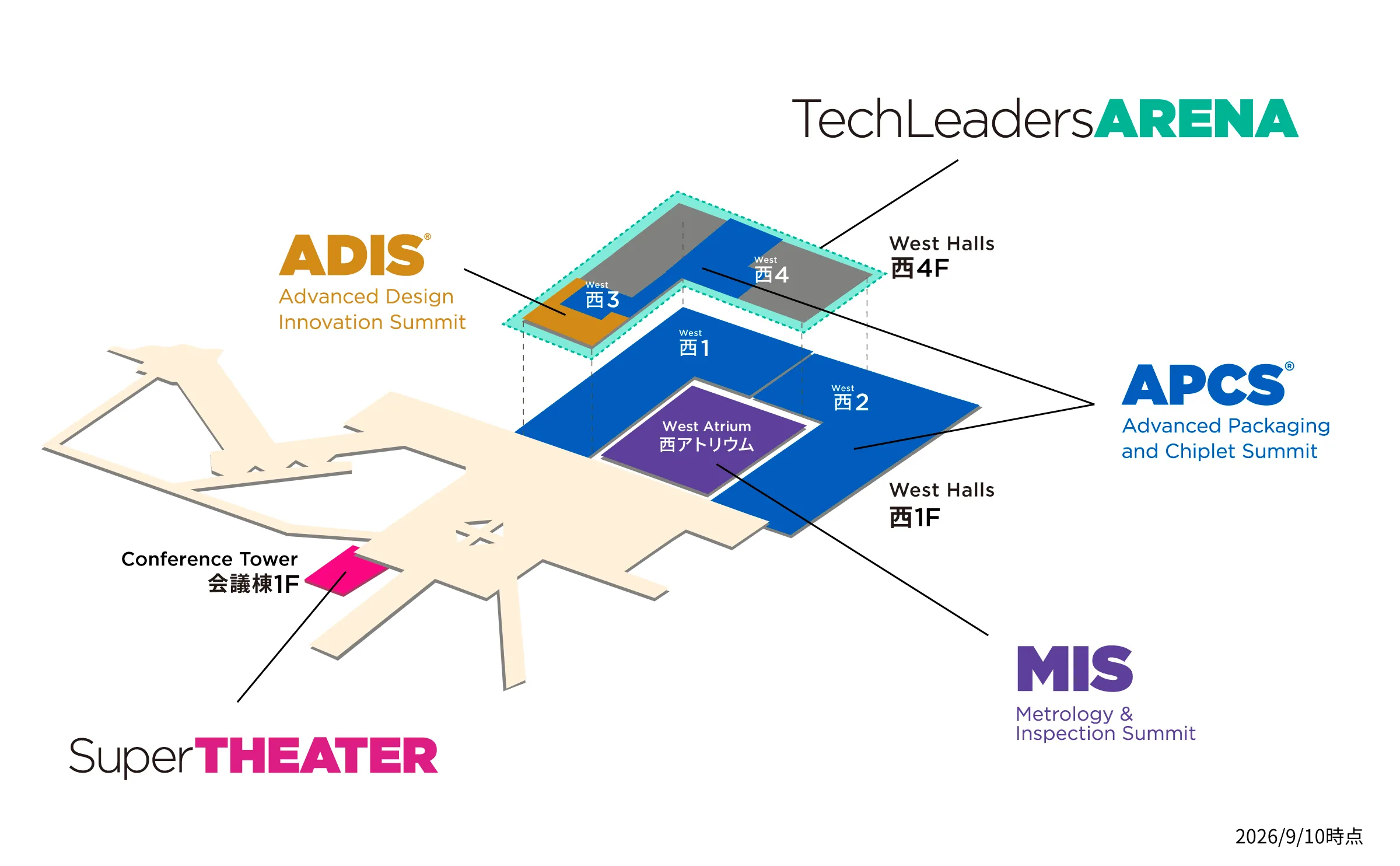
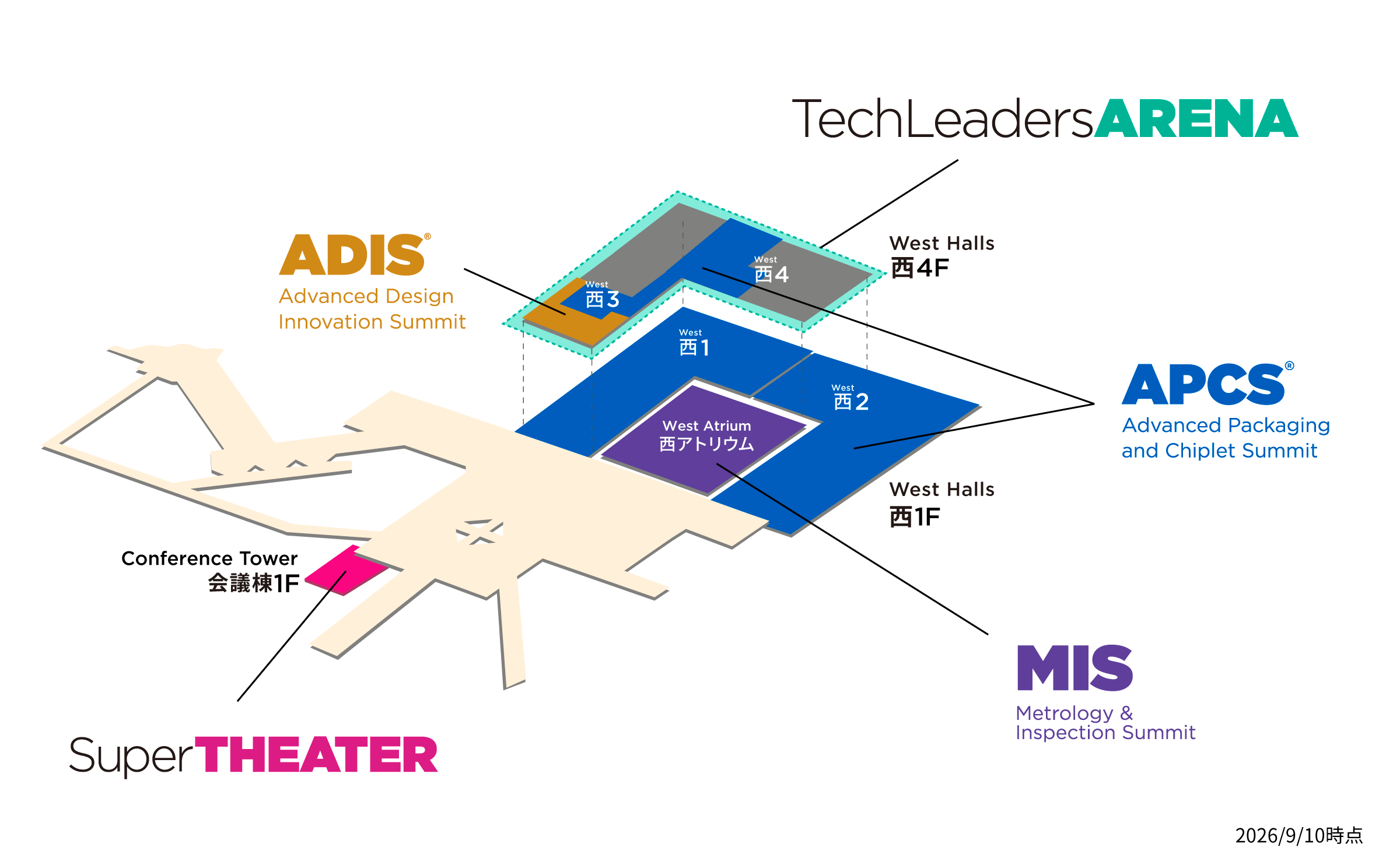
A new spotlight area focused on inspection and measurement technologies supporting semiconductor manufacturing. We will showcase innovative solutions from various companies in West Hall 1F West Atrium.
Conference
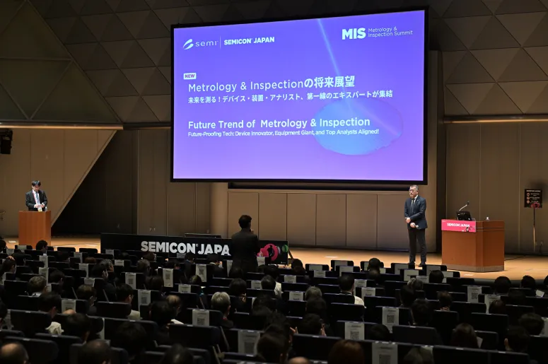
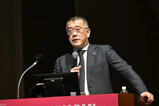
MIS 2026 Seminar Program
- Future Trend of Metrology & Inspection; Frontier Insights from a Device Maker, an Equipment Supplier, and Academia

Networking Event
MIS Networking × STS Metrology / Inspection GETOGETHER × STS Lithography GETOGETHER
Thu., Dec. 11 17:30-18:30
Special Joint Networking Event: MIS Networking, STS Lithography GETOGETHER and STS Metrology / Inspection GETOGETHER
Event Overview
Event Overview
Date
December 9 - 11, 2026
Venue
Tokyo Big Sight
West Hall 1F West Atrium
Access to Tokyo Big Sight
Organizer
SEMI
Concurrent Events
・SEMICON Japan
・APCS(Advanced Packaging and Chiplet Summit)
・ADIS(Advanced Design Innovation Summit)
Committee
Metrology & Inspection Summit Initiatives Committee
Sponsors
