

Welcome to the Design-Driven Era of Semiconductors.
Dec 17 to 19, 2025 | Tokyo Big Sight
What is Advanced Design Innovation Summit?
Welcome to the Design-Driven Era of Semiconductors.
The importance of semiconductors and software in developing systems continues to grow.We are entering an era where critical semiconductors are no longer just purchased, but manufactured in-house.
The semiconductor design field is also evolving rapidly, with advancements in EDA tools (such as AI utilization and digital twins) supporting the growth of the semiconductor design industry.
Here lies discussion offering insights into fundamental challenges: what to design and how to strategically align it with business objectives.
The latest exhibits and networking opportunities from companies involved in EDA, IP, and device/board design will also be provided simultaneously.


Join ADIS
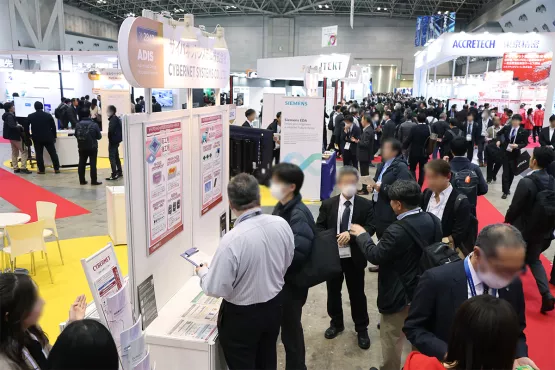
Exhibition
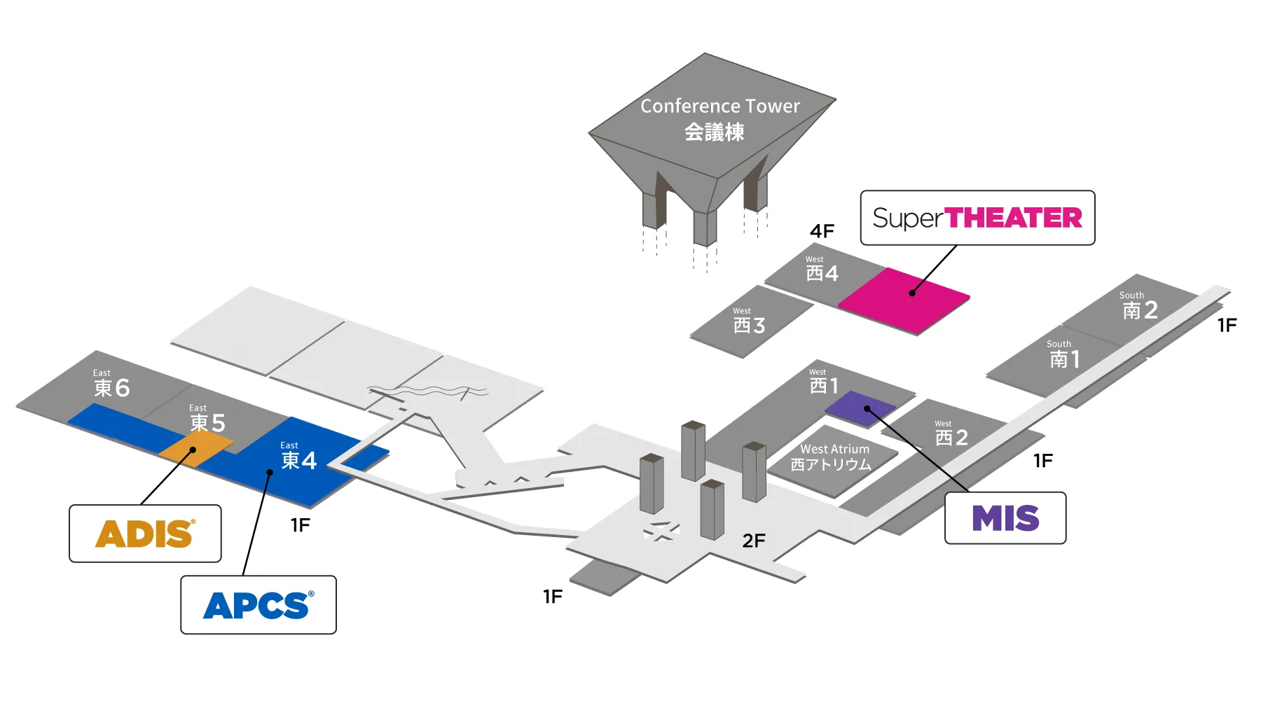
This year's ADIS exhibition area will be in East Hall 5.Industry-leading companies and organizations will showcase their latest technologies, solutions, and services.
Exhibits will feature the latest software (EDA, IP, digital twin-related, etc.), AI semiconductor devices, and printed circuit boards.
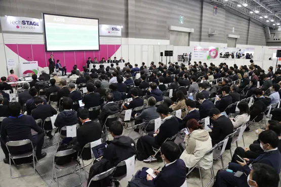
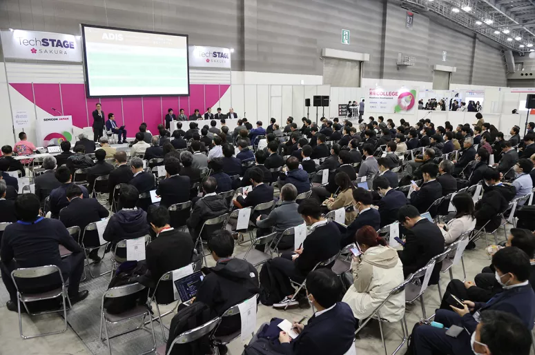
Conference
Three conferences will be held on Thursday, December 18th:
① AI + Digital Twins: Shaping the Future of Design
② Latest Trends in CPU・Processors for the Embedded and IoT Industries
③ The Supercomputer “Fugaku” Development Project

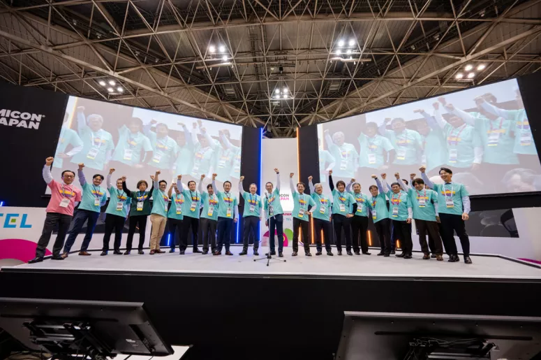
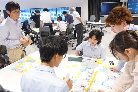
APCS & ADIS Networking
Last year's networking event (invitation-only) was well-attended by many participants.
As in previous years, we will host a networking session that includes attendees of the APCS (Advanced Packaging and Chiplet Summit) in the advanced packaging and packaging fields.
Exhibitors from the APCS and ADIS exhibition areas, speakers, and members of both the APCS and ADIS committees are expected to participate.
Educational course
This is only Japanese event. See below in Japanese.
Event Overview
Event Overview
Date
December 17 - 19, 2025
Venue
Tokyo Big Sight
East Hall 5
Access to Tokyo Big Sight
Organizer
SEMI
Concurrent Events
- SEMICON Japan
- APCS(Advanced Packaging and Chiplet Summit)
- MIS(Metrology &Inspection Summit)
Committee
ADIS (Advanced Design Innovation Summit) Initiatives Committee
