STS Advanced Device Process Session
Semiconductor Technology that Opens the Future: The Challenge of High Performance and Energy Efficiency
Conference Tower 607 / Online (Zoom)


Fee (Exclusive of tax)
- Per Session : SEMI Members 10,000JPY / Non-Members 20,000JPY
- STS 1 Day Pass : SEMI Members 27,000JPY / Non-Members 54,000JPY
*Above fee includes "Download Presentation Materials" (some presentation materials might be written in Japanese)
*Please note that there are separate tickets for in-person and online participation.
Semiconductor devices are driving waves of technological innovation in a wide range of fields, including mobile, IoT, HPC, and the automotive industry, and are transforming our daily lives. At the same time, the increase in energy consumption and environmental impact caused by high-performance devices presents new challenges, and the development of energy-efficient devices is an urgent issue. In this lecture, we will explain the latest logic and memory device technologies and innovative approaches to addressing these issues.
< SEMI Technology Symposium (STS) >
This first technology seminar series in SEMICON Japan founded in 1982, now grown to the international tech symposium marks the 43rd this year. It has been developed as a place to discuss technology among engineers by picking-up the semiconductor technology trends and its issue and sharing the practical technologies to the industry. This symposium stimulates global business growth by involving a variety of different players and visitors.
This program is organized thanks to "SEMI Technology Steering Committee (STS)" formed by top engineers from industry-leading companies, universities, and research institutions.
Program Agenda
Session Chairs: *In alphabetical order by company name
Isao Nambu (EBARA), Junichi Mitani (Socionext)
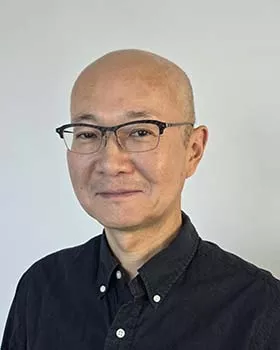
Foundry market growth has been continuously made and recent AI technology accelerates a strong demand in HPC application, which opens tremendous opportunities for the semiconductor industry. There is no doubt that the growth has been led by countless technology innovations, including material/tool/design. Among those evolutions, one of key breakthroughs is Transistor dimension change, like Planer transistor to FinFET. The dimension change can creates not only tremendous Power/Performance/Area improvement, but also an additional value for design collaboration (DTCO). Currently the industry is in a transition for another dimension Gate-All-Around (GAA) transistor to make another technology leap and GAA products have been already launched. In this presentation, the advanced logic platform technology in new dimension era will be introduced.
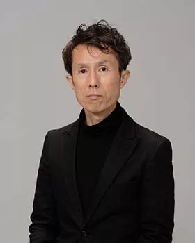
Flash memory is a very simple device consisting of floating gate transistors connected in series. Because of its simplicity, flash memory was the first among all semiconductor memories to reach the technological limit of high density by miniaturization in a plane. 3D flash memory broke through the technological limits of conventional flash memory by stacking many MONOS-type transistors and continued to further increase the memory density. Today, ultra-high memory density has been achieved to a level where 256 gigabytes of digital data can be stored on a single chip of only 1 cm2 in size. In recent years, following flash memory, 3D technology has been actively studied in DRAM and logic devices. In this presentation, I will introduce technical issues and countermeasures for high stacking of 3D flash memory. In addition, Moore's law has been promoted against the background of the scaling law. On the other hand, the scaling law does not hold true for densely stacked memory, and a new technical challenge has revealed for increasing speed. In this presentation, I will introduce the issues and countermeasures for high-speed improvement caused by the high stacking density of 3D flash memory.
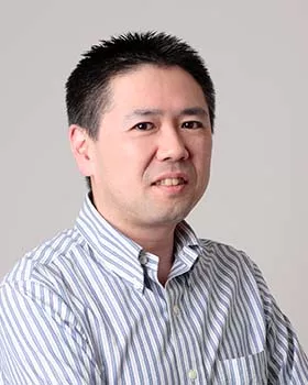
This presentation overviews memory centric AI accelerators and computing for AI applications. To resolve the Von Neumann bottleneck, data movement should be minimized. CiM, Computation-in-Memory technogy achives the processing and memory functions such as MAC functions by a single memory cell. As a reculst, the extremely low power, high performance and low cost AI caclutation is realized.
For those who would join this event, please come to the venue (TBA by begining of November) around 5 PM.
*Please note that a visitor badge is required to enter this event, even though no application is needed in advance.