STS Packaging Session
Chiplet Packaging Technologies
Conference Tower 607 / Online (Zoom)


Fee (Exclusive of tax)
- Per Session:SEMI Members 10,000JPY / Non-Members 20,000JPY
- STS 1 Day Pass:SEMI Members 27,000JPY / Non-Members 54,000JPY
*Above fee includes "Download Presentation Materials" (some presentation materials might be written in Japanese)
*Please note that there are separate tickets for in-person and online participation.
High-end CPUs/GPUs will require the large-scale Heterogenous Integration and the chiplet configuration. New packaging processes and Jisso technologies will be important.
< SEMI Technology Symposium (STS) >
This first technology seminar series in SEMICON Japan founded in 1982, now grown to the international tech symposium marks the 43rd this year. It has been developed as a place to discuss technology among engineers by picking-up the semiconductor technology trends and its issue and sharing the practical technologies to the industry. This symposium stimulates global business growth by involving a variety of different players and visitors.
This program is organized thanks to "SEMI Technology Steering Committee (STS)" formed by top engineers from industry-leading companies, universities, and research institutions.
Program Agenda
*Please note that the program may be subject to change.
Session Chairs: *In alphabetical order by company name
Haruo Shimamoto (Advanced Industrial Science and Technology), Kazunori Kato (Advanced Interface Technology), Shoji Uegaki (Crane Research), Yoshihiro Tomita (Intel), Noboru Hayasaka (TOWA)
President
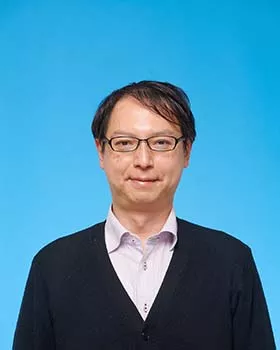
With the demise of Moore's law, chiplet integration technology is expected to become a technology to realize heterogeneous integration as typified by the scale-out of device integration scale and the elimination of the von Neumann bottleneck, and actual implementation has begun. The background and the future of this technology will be discussed, taking into account the current research status.
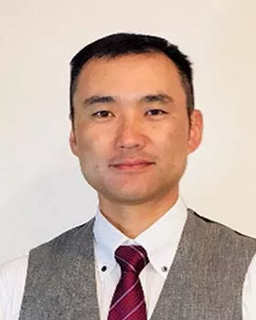
In recent semiconductor technology, Moore's Law has reached a plateau, and 3D integration is essential as a measure to further improve the degree of integration. Hybrid bonding as a new bonding (chip/wafer stacking) technology would be great promising. Inorganic materials that have been put to practical use as insulating materials are currently being considered. In this presentation, we will focus on polymer materials due to yield improvement at low-temperature processes.
*Please note this presentation will not be broadcasted to the online attendees.
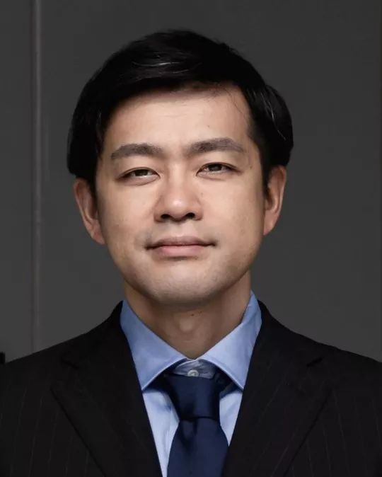
TSMC CoWoS is becoming an indispensable technology for future evolution of HPC such as generative AI. Ever-growing challenges in packaging process and material are expected as substrate size and thermal design power increase continues. TSMC Japan 3DIC R&D Center is driving future material pathfinding for CoWoS, together with partners in Japan. In this talk, latest progress and future outlook are discussed.
After the session, please stay for more discussion where ask questions directly to the speakers and other participants besides exchange greetings as well as name cards.