Overview of Back-End Processes for Young Engineers I
A Must-Have for Young Semiconductor Engineers! Seminar on the Latest Packaging Technology that Supports Next-Generation Semiconductors
Conference Tower 606
 *JAPANESE ONLY PROGRAM
Fee (Exclusive of tax) :
- Per Session SEMI Members 10,000JPY / Non-Members 20,000JPY
- 1 Day Pass SEMI Members 25,000JPY / Non-Members 50,000JPY [Overview of Back-end Processes for Young Engineers I / II]
*Above Fee Includes
- Right to attend the APCS/ADIS Networking Party on 12/12(Wed.) *Students are Not Allowed
- Luch box for applicants of 1 day pass
**Presentation Materials will not be distributed.
This two-part session, divided into morning and afternoon, will cover a wide range of topics from the basics of semiconductor packaging to the latest technologies, which holds the key to the future evolution and development of semiconductors.
In the morning session, we will focus on the history and overview of semiconductor back-end processing.
In addition, those attending this session can also participate in the APCS/ADIS networking event* (12/12), where you can interact with key people working on advanced packaging technology.
*As this event will serve alcohol, students are not allowed to attend.
Program Agenda
*Please note that the program may be subject to change.
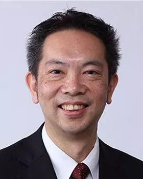
概要:TBA
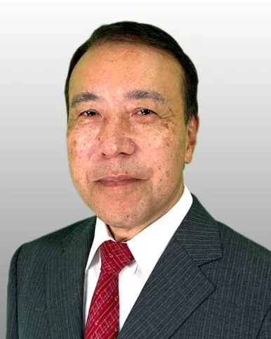
Lecturer
In this section, I will talk about an overview of each post-processing flow following the wafer is completed, explaining each of the conventional steps such as wafer testing, back grinding, dicing, die bonding, wire bonding, resin sealing, outer lead plating, terminal processing, marking, and shipping test. I will explain each of the conventional steps and also introduce the basics, including the currently common flip chip and BGA connection methods.