
For top players in semiconductor
packaging and PCB assembly
Dec 9 to 11, 2026 | Tokyo Big Sight
What is Advanced Packaging and Chiplet Summit?
Semiconductor packaging requirements vary depending on the application—ranging from miniaturization and low power consumption to high reliability and cost efficiency.
To meet these diverse needs, a wide range of technologies continues to evolve through constant innovation and challenge.
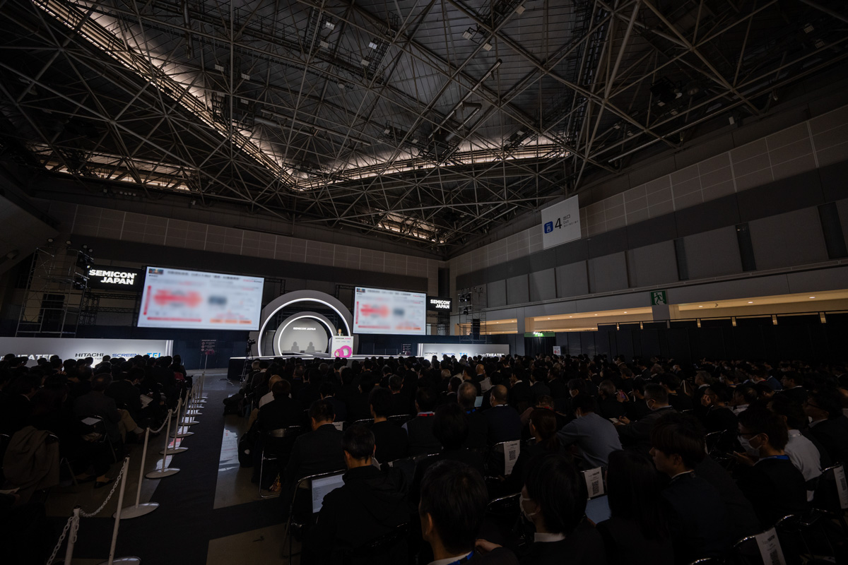
Launched in 2022, the Advanced Packaging and Chiplet Summit (APCS) features a conference focused on the latest industry trends, an exhibition area showcasing cutting-edge technologies and solutions, networking opportunities with VIPs and key industry figures, and educational sessions covering everything from packaging fundamentals to the latest advancements.
This summit serves as a platform to accelerate the growth of Japan’s advanced packaging and chiplet ecosystem, offering participants valuable insights and practical takeaways.
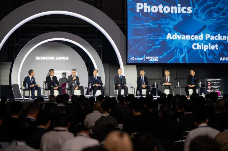

Join APCS
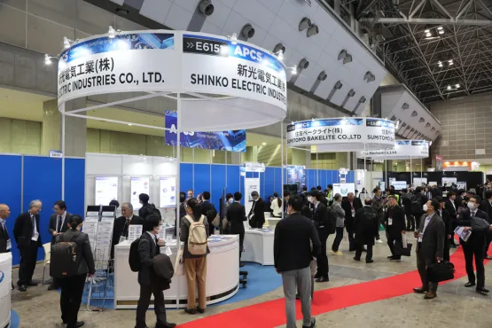
Exhibition
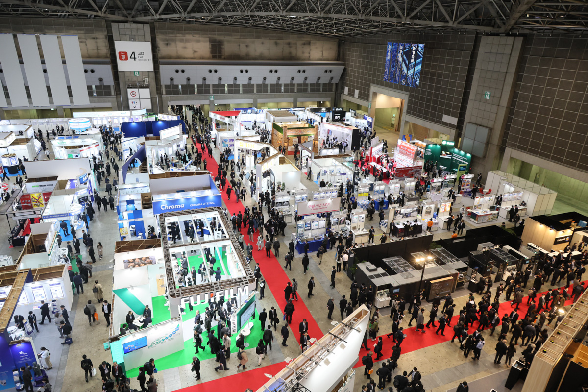
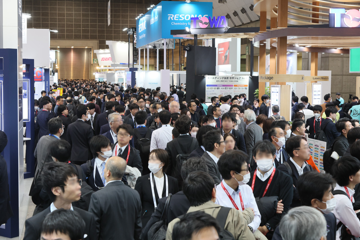
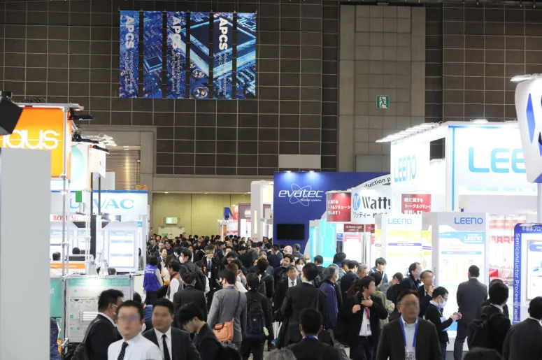
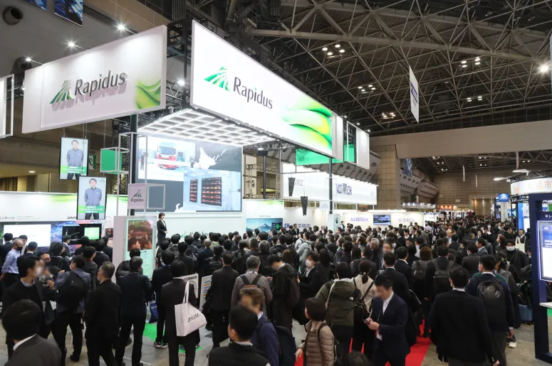
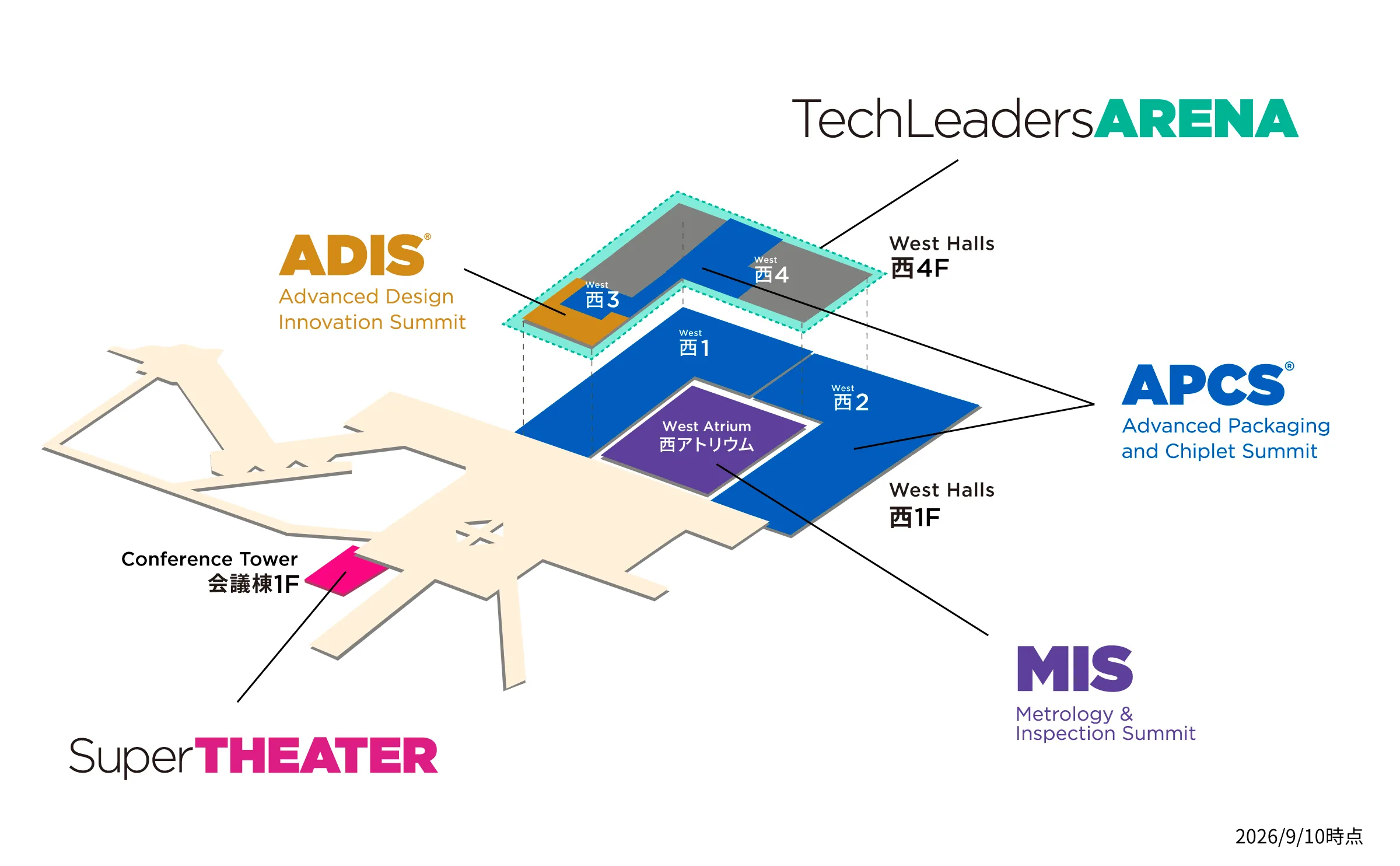
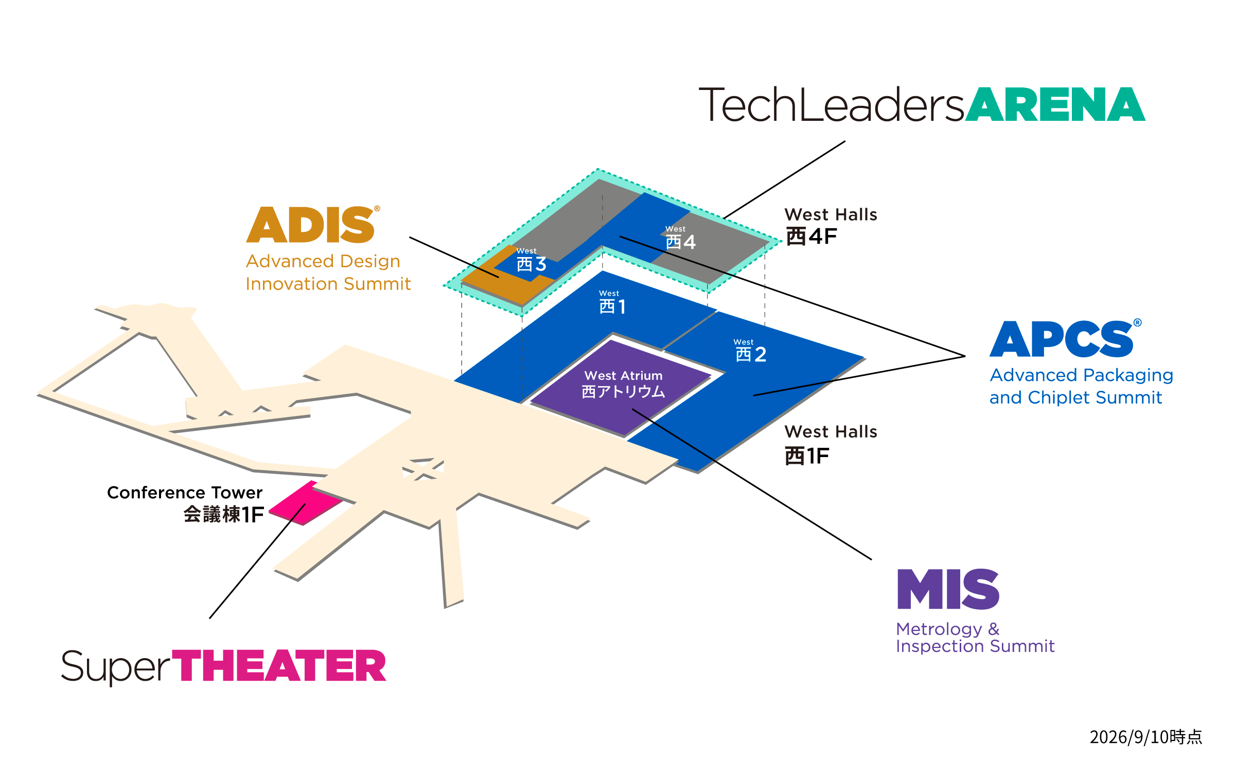
This year’s APCS exhibition will be held in East Halls 4–6, featuring leading companies and organizations showcasing the latest technologies and solutions.
As design becomes increasingly critical in advanced packaging and chiplet development, the ADIS (Advanced Design Innovation Summit) exhibition area—focused on design and verification—will be located adjacent to APCS in East Hall 5. We encourage you to explore both exhibition areas together.
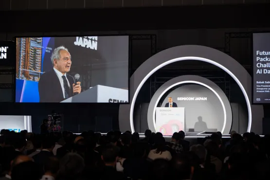
Conference
Chiplets Connecting the Future, Transforming Society.
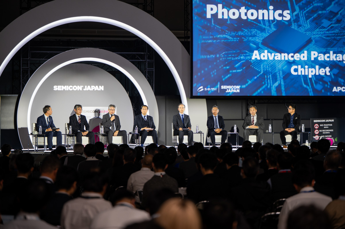
Toward a sustainable future shaped by photonics, mobility, and AI, APCS explores the future of advanced packaging through five sessions: substrate innovation, thermal-stress management, photonic-electronic integration, and next-gen manufacturing led by young engineers.
APCS 2025 Conference Programs
・Advanced Packaging Chiplet Summit 2025
Chiplets Connecting the Future: Photonics, Mobility, and AI Shaping a Sustainable Society
・APCS Technology SessionⅠ Advanced Package Substrates
・APCS Technology Session Ⅱ Thermal and Stress Management
・APCS Technology Session Ⅲ Photonic-Electronic Integration
・APCS-Next Session Innovations in AI, Semiconductors, and Digital Twins

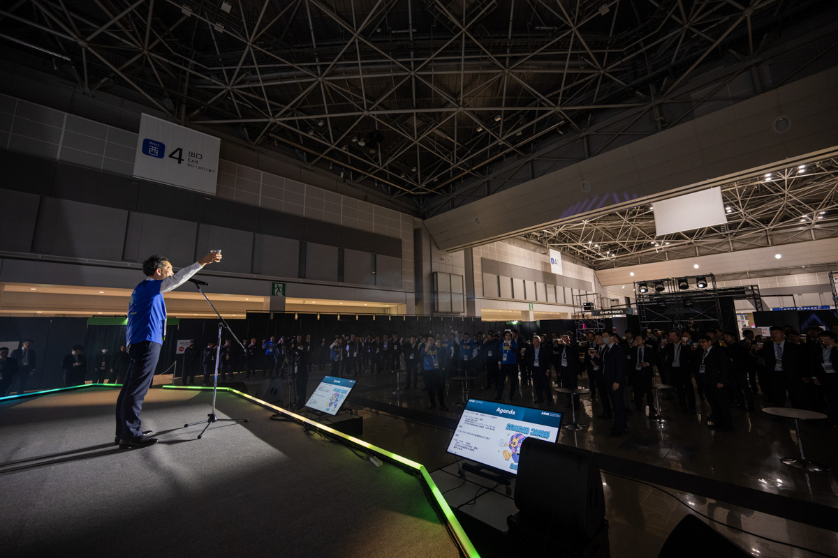
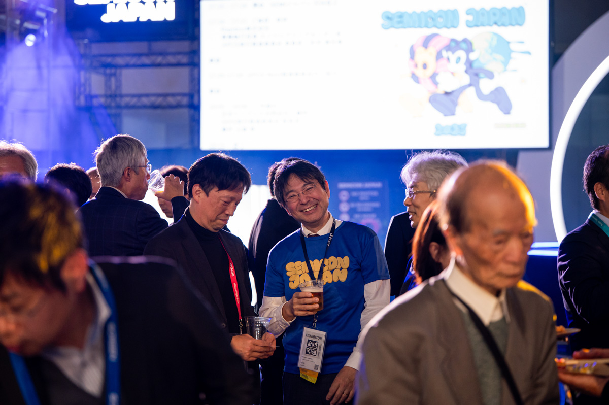
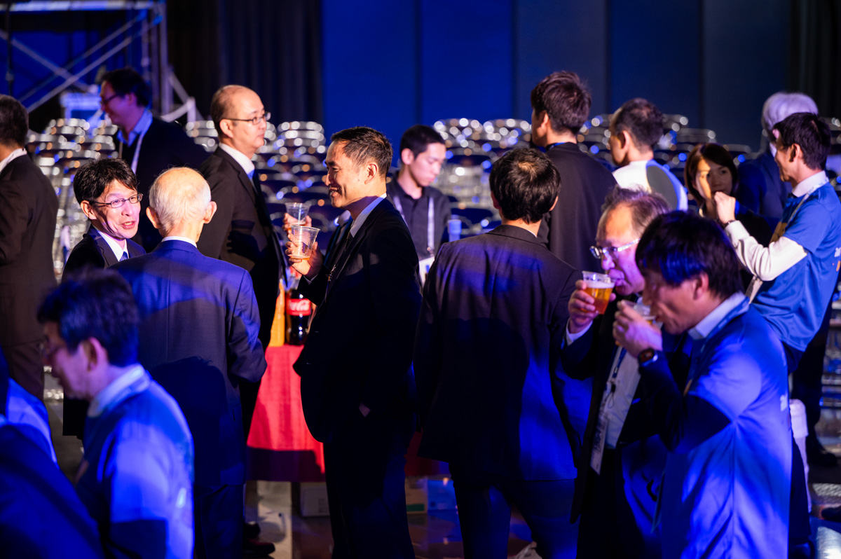
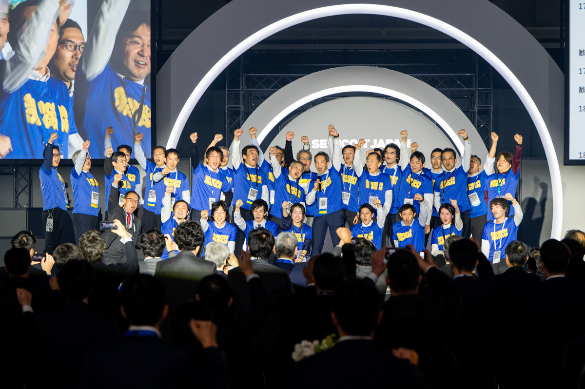
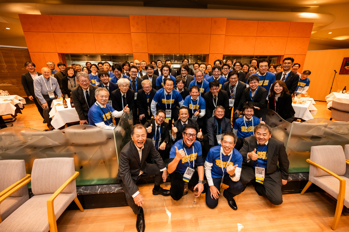
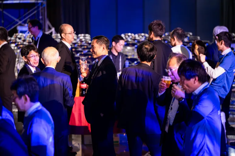
APCS & ADIS Networking Event
Following last year’s success, the invitation-only networking event will be held again this year.
This time, the event will expand to include participants from ADIS (Advanced Design Innovation Summit), which focuses on semiconductor design and verification. Exhibitors, speakers, and committee members from both APCS and ADIS are expected to attend.
It will be a valuable opportunity to build cross-disciplinary connections—don’t miss it.
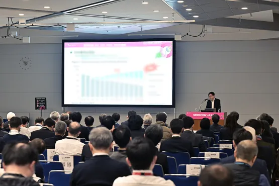
Educational course
We will provide a comprehensive overview of semiconductor packaging—from fundamental concepts that underpin the evolution and advancement of semiconductors to the latest cutting-edge technologies—divided into two sessions in the morning and afternoon.
2025 Educational Courses
・Overview of Back-end Processes for Early Carrer Engineers I
・Overview of Back-end Processes for Early Carrer EngineersⅡ
Event Overview
Event Overview
Date
December 9 - 11, 2026
Venue
Tokyo Big Sight
Organizer
SEMI
Concurrent Events
・SEMICON Japan
・ADIS(Advanced Design Innovation Summit)
・MIS(Metrology & Inspection Summit)
Committee
Sponsors








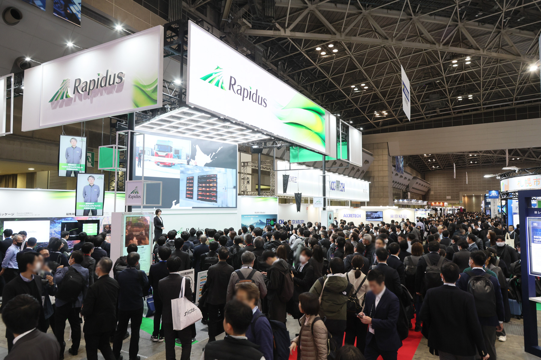
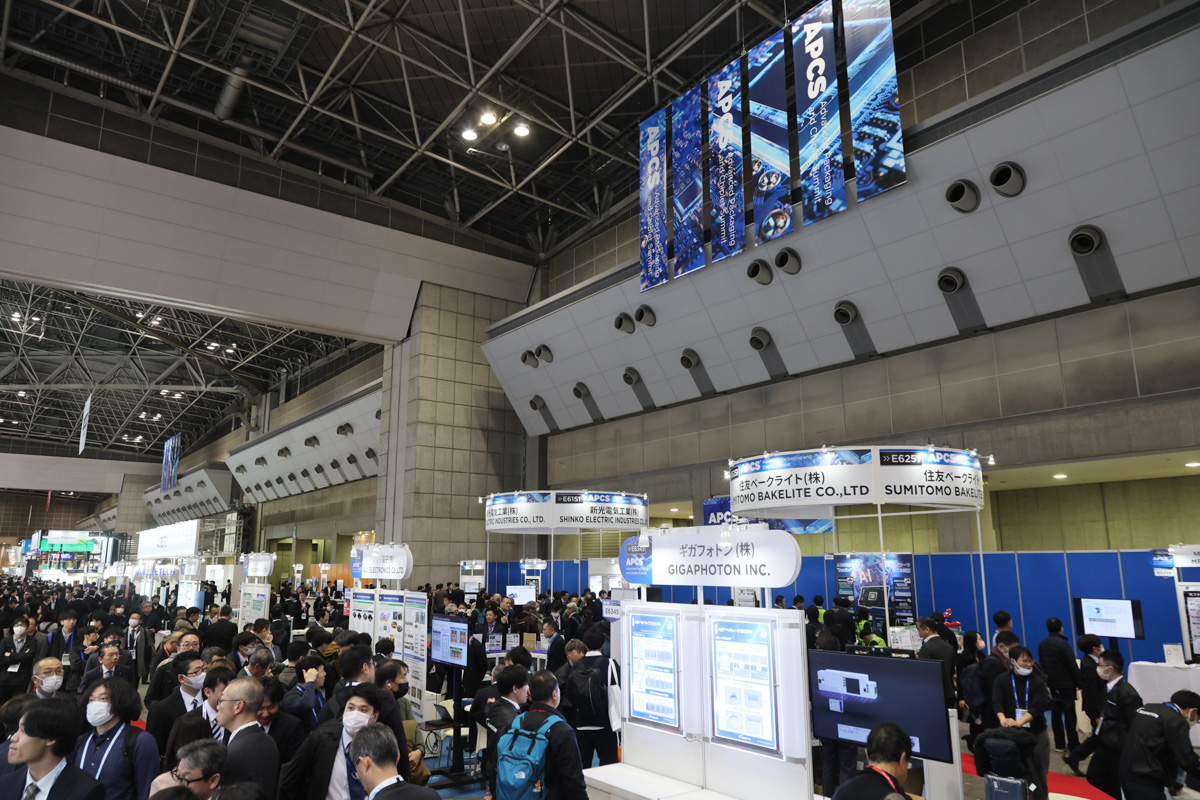
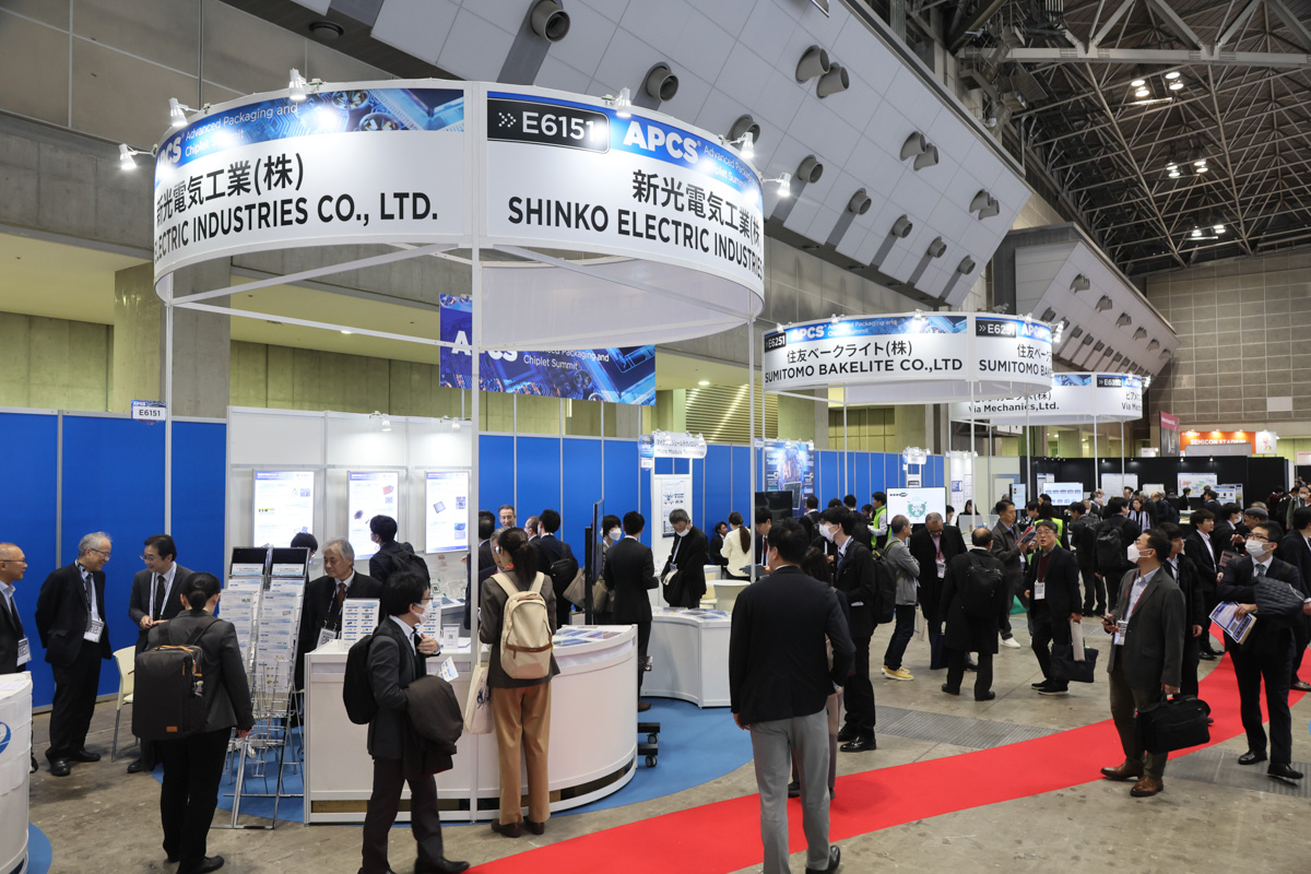
APCS 2025 Photo Gallery
Please mention the source "SEMI" to use the following photos.