
Exhibits covers the entire semiconductor manufacturing process

SEMICON Japan is a premium international exhibition for the electronics manufacturing supply chain, covering manufacturing technologies, equipment, and materials in the semiconductor industry, as well as SMART applications such as cars and IoT devices.
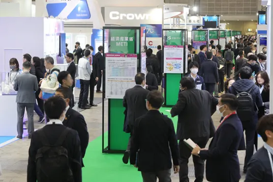
More than 1,200 companies and organizations are set to showcase their booths, spanning every stage of the semiconductor manufacturing process. This year’s event is expected to surpass last year’s in scale and scope.
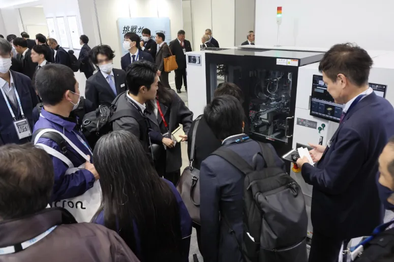
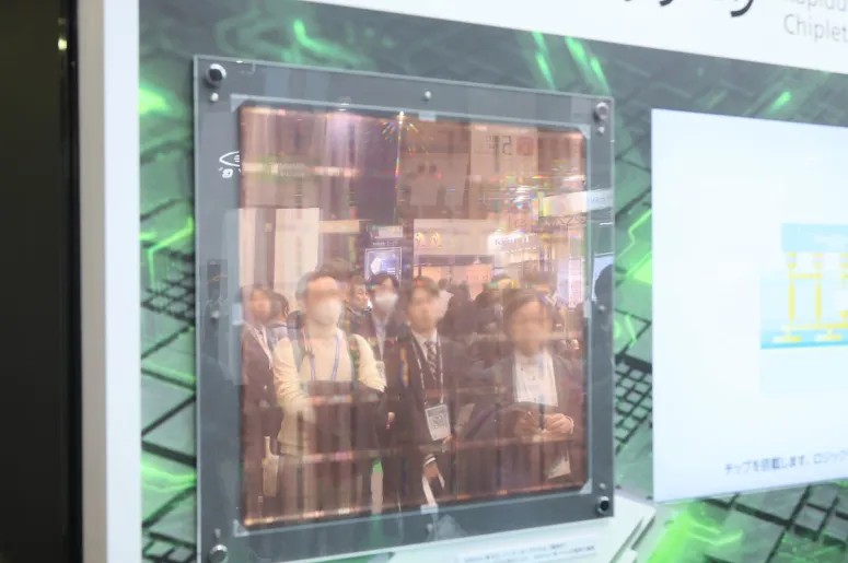
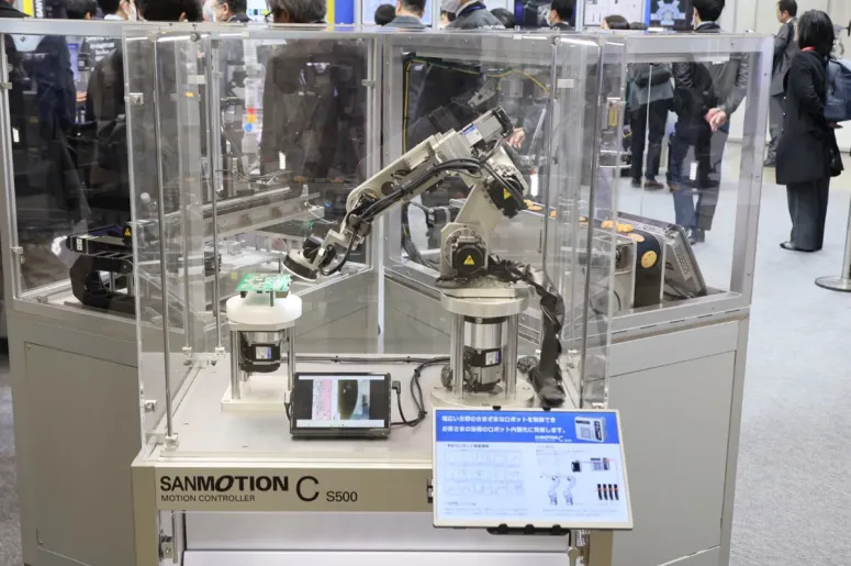
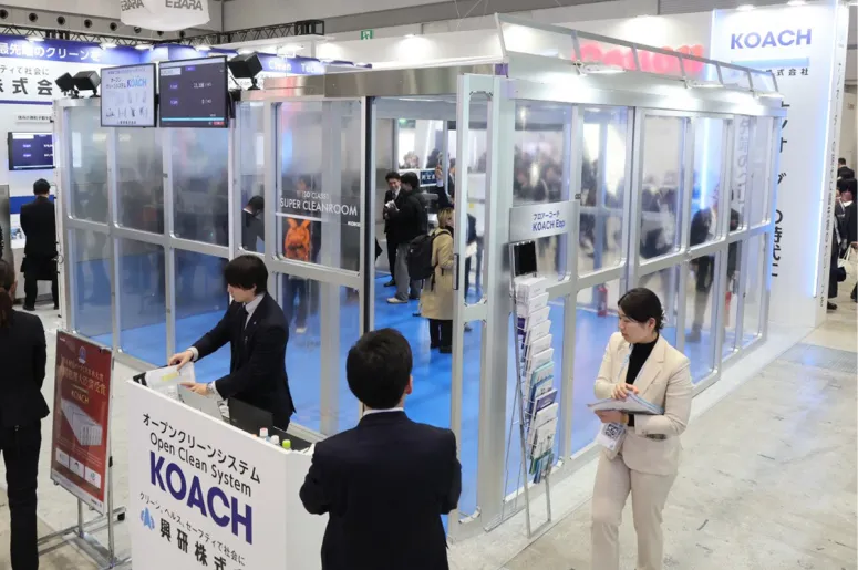
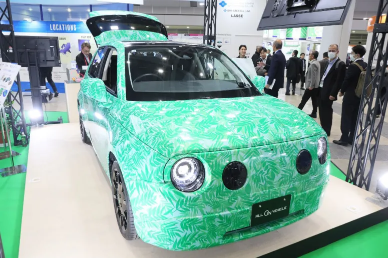
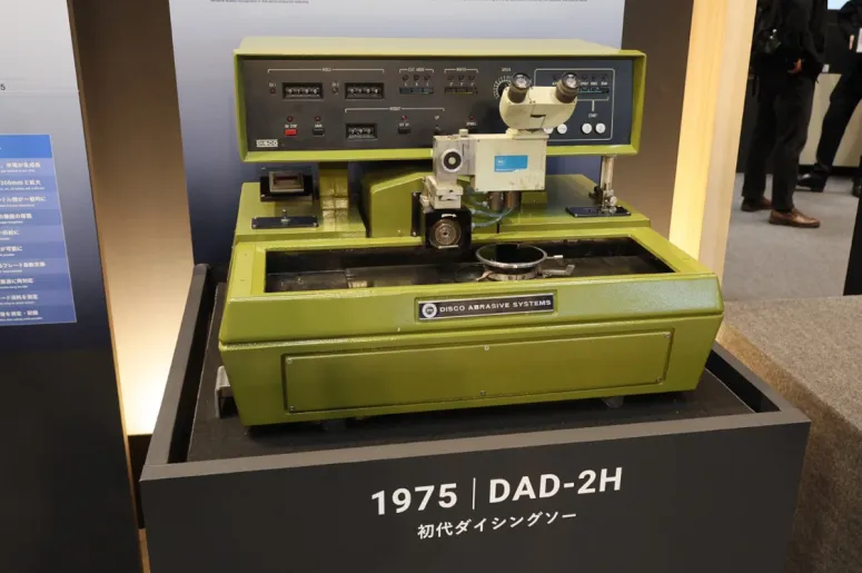
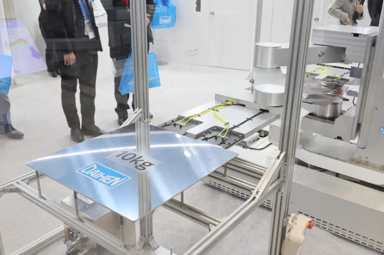
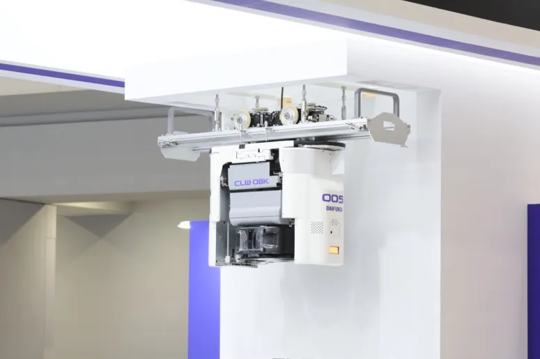
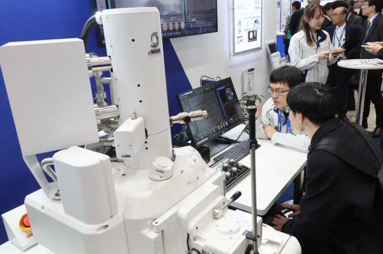
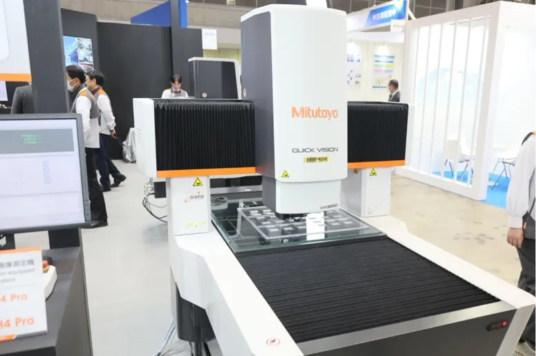
Exhibit Overview & Floor Map
Explore the venue layout and exhibition zones ahead of your visit with the SEMICON Japan floor map.
Planning your route in advance and locating key exhibitors and pavilions will help you maximize your time and get the most out of your SEMICON Japan experience.
- TechLeadersARENA | West Hall 3, 4
- Advanced Packaging and Chiplet Summit(APCS)| West Hall 3, 4
- Advanced Design Innovation Summit(ADIS)| West Hall 3
- AI x Sustainability x Semiconductor Summit | West Hall 4
- Metrology & Inspection Summit(MIS)| West Atrium
*Information as of 2025.
A wide variety of special exhibits that give visitors a sense of the "future"
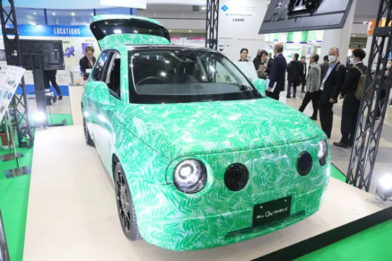
Technology Pavilion
Explore technology pavilions showcasing the latest innovations in the semiconductor industry, including quantum technologies, power electronics, GaN, AI, smart manufacturing, and advanced device teardown exhibits.
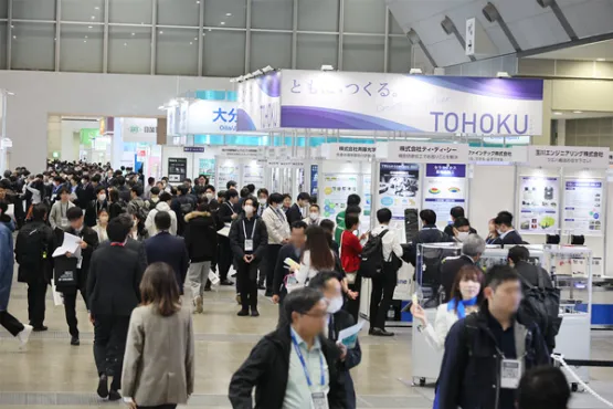
Regional Pavilions
Explore regional pavilions from Japan and around the world, showcasing the latest technologies and industry development initiatives from companies and organizations supporting the semiconductor ecosystem.
SEMICON PATHs
An exhibition area connecting the past, present, and future of the semiconductor industry. Explore market trends, industry developments, and the history of semiconductor technology through easy-to-understand displays.
Concurrent Events