
Monday, November 21, 2022
Future of Semiconductor Technology Evolving Through Fusion of Front-end and Back-end Processes According to Global Leaders
Japanese Original Version was written by Motoaki Ito, Enlight,Inc.
Translation by SEMI Japan
A special exhibition dedicated to back-end technology, entitled “Advanced Packaging and Chiplet Summit (APCS),” will be collocated with SEMICON Japan 2022 on December 14–16, 2022 at Tokyo Big Sight.
SEMICON Japan has focused primary on the front-end processing for semiconductors. Of course, the past events also included exhibits and lectures concerning the back-end processing in the semiconductor industry. Given that back-end processes are strongly linked to system technology, however, many of you must have had to collect information also from exhibitions other than SEMICON in order to keep up with the latest industry trends.
Traditionally, the roles of front-end and back-end semiconductor manufacturing processes have been clearly divided. This means that developing technology in one did not really require understanding trends in the other. Now, however, Yasumitsu Orii (Executive Officer, NAGASE), who acts as Chairman of the APCS Initiatives Committee says: “Expanded use of chiplet technology, which is an essential element of further miniaturization and integration, has resulted in global wiring, which has traditionally been formed inside chips, becoming transferred to the substrate side of packages. This means that technological innovation is happening across the boundaries between front-end and back-end processes. In other words, we are entering a phase where we need to create a fusion of, and redefine, the roles of front-end and back-end processes to allow semiconductor technology and business to grow further in the future. It is now necessary for those involved in front-end processing to keep up with the latest back-end processing trends, and for those involved in back-end processing to keep up with the latest front-end processing trends, while having seamless discussions with each other.”
We can no longer talk about the latest front-end processing unless we know about the latest back-end processing. For example, TSMC, which owns the world’s most advanced front-end processing technology and leads the world as a contract chip manufacturer, is also known as a company that places the greatest emphasis on the development of back-end technology and business. Over the past ten years or so, it has been focusing on new back-end technologies called Integrated Fan-Out (InFO) and Chip-on-Wafer-on-Substrate (CoWoS) (Figure 1). Its customers including AMD, NVIDIA, Xilinx and Apple have substantially increased their business competitiveness by taking advantage of its chiplet technology based on these technologies. If TSMC had viewed back-end processing as out of its realm, the competitiveness which the company and its customers enjoy at present would not have been possible.
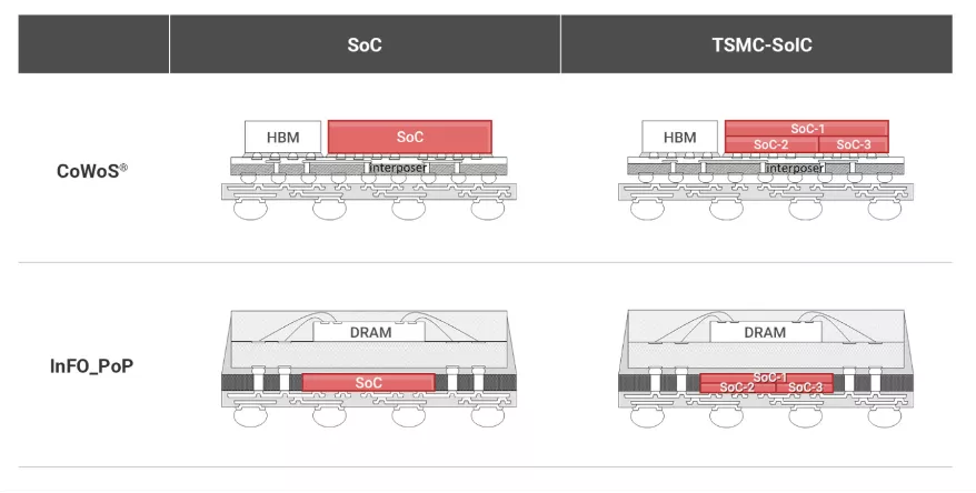
Figure 1: InFO and CoWoS, back-end technologies that support the competitiveness of TSMC
Source: TSMC
Japan is a suitable place to discuss the evolution of leading-edge back-end technology
While many SEMICON events are held in different parts of the world, APCS is an exhibition specializing in back-end technology, which Japan has decided to implement ahead of the rest of the world. However, it is natural that Japan would become the first to host this kind of event because the country has a favorable environment to produce back-end technological innovations, perhaps even better than the US and Taiwan. Japan is home to printed-circuit board manufacturers with the world’s leading technological expertise, including IBIDEN, Kyocera and Shinko Electric Industries, in addition to many companies that provide materials and devices for the development and utilization of the most advanced back-end technology. As such, Japan can be said to be the most suitable place to discuss the future evolution of leading-edge back-end technology.
There has not been much progress in the development of advanced front-end technology in Japan for many years now, except for some companies. In fact, Japan does not have many engineers who can create leading-edge front-end processes like those utilizing EUV lithography. Even so, wiring on chiplet substrates is usually installed in micron order using KrF lithographic exposure. At the same time, there is a technological need, different from in front-end processes, to carry out minute wiring on different materials at low cost, such as printed and glass substrates with a large area of 500 mm or 600 mm, not 300 mm silicon wafers. The most advanced lithographic exposure technology peculiar to back-end processes is highly sought after in this field, in which there are plenty of opportunities for Japanese engineers to demonstrate their expertise.
Back-end technological innovations wanted by companies utilizing leading-edge front-end technology
According to Chairman Orii, “the concurrent implementation of SEMICON, which provides the latest information about advanced front-end technology, and APCS, which brings together information about the world’s leading back-end technology, has profound significance.” This is because the information on front-end technology that can be collected at SEMICON and the information on back-end technology to be provided at APCS can be of great value to people working in back-end and front-end processes, respectively, in considering their own technological development and business strategies. As with SEMICON Japan, APCS also invites world-class high-level speakers to its many lectures and seminars. If you carefully collect information during this three-day event, you can efficiently and comprehensively gather information on technological innovations happening across the boundaries between front-end and back-end processes, as well as on the latest business trends.
The Advanced Packaging and Chiplet Summit 2022: The Future of Packaging by Global Leaders, which will be held on Thursday, December 15, at SuperTHEATER, set up in East Hall 2, will bring together global leaders leading the most advanced semiconductor development to talk about the evolution and applications of semiconductor technology promoted through fusion of front-end and back-end processes.
From Intel, Ravi Mahajan, Fellow, will give a lecture. Under the title “Challenges and Opportunities in Heterogeneous Integration using Chiplets,” he will talk about the evolution of computing projected to be achieved through chiplet-based heterogeneous integration technology. This lecture is also planned to include the latest information on UCle, a standard for chiplets led by Intel.
From AMD, which was early to introduce chiplet technology and has achieved a quantum leap in its CPU business, Mark Fuselier, Senior Vice President, AMD Technology & Product Engineering, will deliver a lecture. The focus of his lecture, entitled “Supporting the Future of High-Performance Computing,” is on the innovations required to be realized in the coming ten years for continued evolution of high-performance computing (HPC) in the future.
Another lecturer is Rama Divakaruni from IBM, who is an IBM Research Distinguished Engineer. Under the title “Evolving AI Models and Implications to Semiconductor Technology,” he will talk mainly about the co-location of memory and logic on modules that supports further evolution of artificial intelligence. IBM is a partner company of the Japanese government that jointly carries out technological development work concerning Step 2: Beyond 2nm, which is the second stage of the government’s semiconductor strategy that aims to rebuild the Japanese semiconductor industry.
From Nippon Telegraph and Telephone Corporation, Hirokazu Takenouchi, Vice President of Device Technology Laboratories, will give a lecture entitled “Photonics-electronics convergence device technology in the IOWN vision.” The IWON vision forms the core of Step 2, the final stage of Japan’s semiconductor strategy. He will provide an outline of photonics-electronics convergence device technology, which can bring reform to the areas of networking and computing.
Besides this program, Japanese and Taiwanese companies, universities, and research institutes will share the latest information on back-end technology through Tech & Biz, a program that provides the latest information on technological developments and business trends in different fields, and SEMI Technology Symposium (STS), an international tech symposium covering the latest developments in semiconductor manufacturing. For example, a speaker from Fujitsu will talk about the supercomputer Fugaku and expectations on packaging technology toward next-generation devices in a Tech & Biz session entitled “Next Generation Computing and Device & Packaging Development in Japan and Taiwan,” which will take place at 605+606, Conference Tower, on Wednesday, December 14. In this session, a speaker from the Industrial Technology Research Institute (ITRI) in Taiwan will also share their latest wide-bandgap semiconductor development results, such as GaN and SiC, and introduce relevant module technology. In another session, STS Packaging Session: Innovation of the Packaging Technology, will provide programs that allow participants to take a comprehensive glimpse at technological developments and business trends in the area of packaging in a day.
The STS Packaging Session on the first day will be followed by an Author’s Interview session, in which participants can directly communicate with lecturers. On the second day, a networking party will be held after APCS from 5 p.m. at SuperTHEATER, which will be joined not only by speakers but also by committee members and exhibitors. This is sure to offer you a great opportunity to find a path to your future through exchanging business cards and information.

APCS 2022 Conference
Advanced Packaging and Chiplet Summit 2022
The Future of Packaging by Global Leaders
Thu., Dec 15 13:00 - 16:20
East Hall 2, SuperTHEATER
Free
Next Generation Computing and Device & Packaging Development in Japan and Taiwan
Wed., Dec 14 11:30 - 12:30
605+606, Conference Tower
Free
STS Packaging Session
Innovation of the Packaging Technology
Wed., Dec 14 15:00 - 16:30
Venue: Conference Room 607+608, Conference Tower, Tokyo Big Sight / Online (Zoom)
Fee (Exclusive of tax) :
SEMI Members 6,000JPY (*Ticket application valid until Fri. Dec.9 (JST), Thereafter, Non-members price will be applied.)
Non-Members 12,000JPY
*Above Fee Includes
Download Presentation Materials (some presentation materials might be written in Japanese.)
The Latest Trend of Advanced Packaging Technology for Post5G
Fri., Dec 16 14:30 - 16:10
605+606, Conference Tower
Free